From Nuclear Weapons to Microchips: Russia’s Historic Nuclear Laboratory Wins Billion-Ruble Semiconductor Equipment Contract

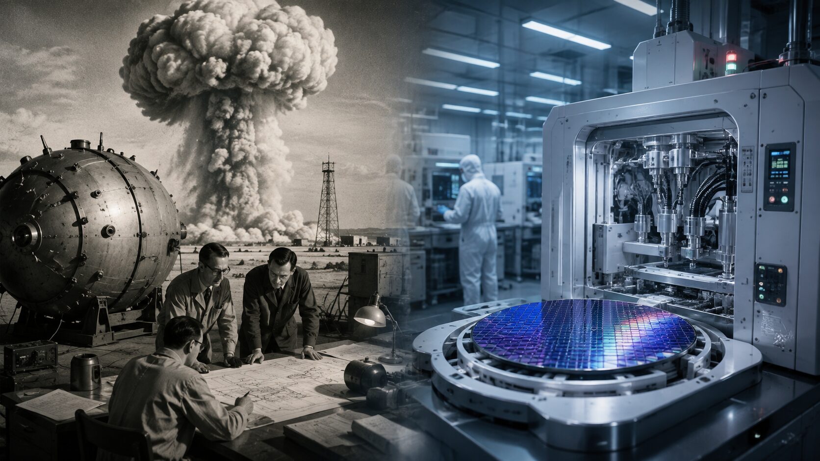
Russia’s Russian Federal Nuclear Center (VNIIEF)—best known as one of the principal developers of the Soviet Union’s first nuclear weapons—has been awarded a major government contract to develop equipment for the country’s semiconductor industry. The Russian Ministry of Industry and Trade has allocated 1.43 billion rubles for the Spray project, which aims to create an automated wet chemical processing system for silicon wafers. Development is scheduled for completion by November 30, 2029.
It is important to clarify one key point: despite some headlines suggesting otherwise, this project is not about building a complete chip manufacturing system or replacing advanced lithography machines. Instead, the new equipment is intended for one specific—but essential—stage of semiconductor fabrication: wet chemical etching and wafer cleaning.
What Exactly Will VNIIEF Build?
The project focuses on developing a fully automated system capable of processing 100 mm, 150 mm, and 200 mm silicon wafers.
According to the technical requirements, the machine will perform several manufacturing operations within a single automated cycle:
- Wet chemical etching
- Surface cleaning
- Wafer rinsing
- Drying
The system is expected to process up to 100 wafers per batch (four standard wafer cassettes), handle multiple chemical reagents automatically, and support SMIF (Standard Mechanical Interface) loading technology, which minimizes contamination by airborne particles.
Why Wet Etching Matters
While lithography machines usually receive the most public attention, chemical processing remains one of the fundamental stages of semiconductor manufacturing.
After circuit patterns are transferred onto a silicon wafer, unwanted material must be removed with extremely high precision.
Wet processing equipment is also used to clean wafers between manufacturing stages and prepare surfaces for subsequent fabrication steps.
Modern semiconductor factories rely on dozens of different types of highly specialized equipment, with lithography representing only one part of a much larger production chain.
Part of Russia’s Import Substitution Strategy
According to the project documentation, most of the system’s critical components must be designed and manufactured domestically.
These include:
- The processing chamber
- Chemical delivery system
- Rotor assembly
- Central control unit
- Control software
Foreign-made components may only be used with explicit approval from the customer. The project is part of Russia’s broader effort to localize semiconductor manufacturing equipment and reduce dependence on imported technologies.
Why VNIIEF?
At first glance, assigning the project to a nuclear weapons laboratory may seem unusual.
In reality, VNIIEF has long expanded beyond its original mission.
The institute possesses extensive expertise in precision engineering, advanced materials, automation systems, scientific instrumentation, and high-technology manufacturing.
In recent years, it has increasingly participated in civilian industrial projects, including semiconductor equipment development.
Only weeks earlier, the institute received another Ministry of Industry and Trade contract worth 992.85 million rubles to develop equipment for wafer bonding and debonding. Combined, the two contracts exceed 2.4 billion rubles.
How Much Will This Help Russia’s Semiconductor Industry?
Developing this type of equipment alone will not make Russia technologically independent in semiconductor manufacturing.
Modern chip production requires an entire ecosystem of sophisticated machinery, including lithography systems, deposition equipment, ion implantation tools, plasma etchers, chemical-mechanical polishing systems, metrology instruments, and many other highly specialized machines.
Nevertheless, localizing even individual manufacturing stages helps reduce dependence on foreign suppliers while gradually building a more complete domestic semiconductor production chain.
That is why the Russian government has recently increased funding for multiple projects aimed at developing indigenous semiconductor manufacturing equipment.
Conclusion
There is undeniable symbolism in the fact that the organization once responsible for developing the Soviet Union’s nuclear deterrent is now working on equipment for semiconductor production.
However, it would be misleading to suggest that VNIIEF is creating a complete chip manufacturing system.
The new project addresses one specific—though highly important—stage of semiconductor fabrication: the wet chemical treatment of silicon wafers. If completed successfully, it will provide Russia’s microelectronics industry with another domestically developed manufacturing tool, representing one more step toward greater technological self-sufficiency, even though many other advanced production systems will still need to be developed.